
Add to Favorites


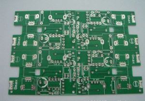
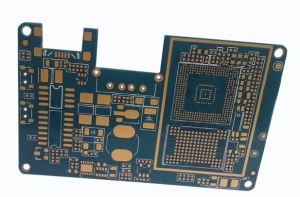
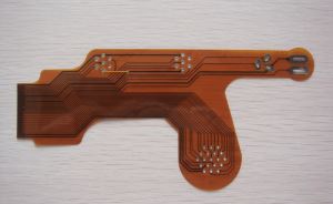
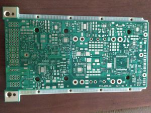
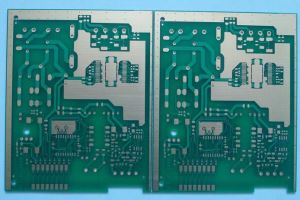
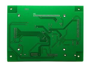
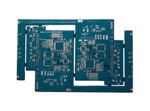
Double Layer Fr4 Tg180 PCB for Telecom Industry
-
Payment


-
Origin
China Mainland
-
Minimum Order
1
-
Packing
Pieces
- Contact Now Start Order
- Description
Product Detail
-
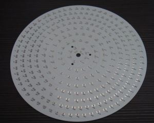
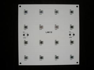
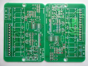
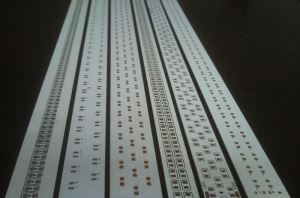
KEDING is well-known as one of the professional double layer fr4 tg180 pcb for telecom industry manufacturers and suppliers in China, which is equipped with one of the famous PCB brands. We can offer you customized double layer fr4 tg180 pcb for telecom industry. Should you want to buy or wholesale our cheap bulk PCB at a discount, please contact us and we also can offer free sample if necessary.
Model NO.:kdpcb-PCB
Type:Rigid Circuit Board
Dielectric:FR-4
Material:Fiberglass Epoxy
Flame Retardant Properties:V0
Mechanical Rigid:Rigid
Processing Technology:Electrolytic Foil
Base Material:Copper
Insulation Materials:Epoxy Resin
Model:FR-4
Trademark:kdpcb
Package:Vacuum Package
Specification:80mm*120mm
Origin:China
HS Code:8534009000
Product Detail
Basic Info
Product Description
1 Specifiction:
Layer: 2L
Material: Fr4
Board thickness: . 1.6mm
Copper thickness: 1oz
Surface treatment: Imersion gold
Application: Consumer electronics
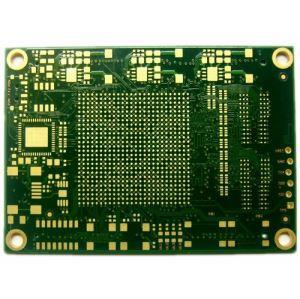
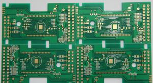
Process capacity
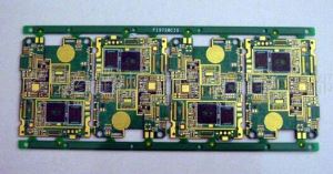
2 We offer:
1~20layers PCB
Aluminum PCB,
Buried/blind via PCB,
High frequency PCB,
3 Why us:
UL, ISO9001/14001, ISO/TS16949 certified.
Staff of 1000+.
19+years experience, annual turnover USD 82Million.
Full-process workshop--more guaranteed quality and lead time
All exported PCB have double-check before sending out.
Layer: 2L
Material: Fr4
Board thickness: . 1.6mm
Copper thickness: 1oz
Surface treatment: Imersion gold
Application: Consumer electronics
Process capacity
| ITEM | PARAMETER | |
| Layers | 1-12L | |
| Material Types | FR-4,FR-4(Middle.High Tg,Halogen Free etc) | |
| Max panel size | 20"×24.5* | |
| Min track width/space for inner layer | 4MIL/4MIL | |
| Min inner layer pad | 4MIL | |
| Inner layer copper thickness | 0.5(MIN)-4 OZ(MAX) | |
| Outer layer Copper thickness | 0.5(MIN)-4 OZ(MAX) | |
| Finished board thickness | 0.4-3.2mm | |
| Tolerance of finished board thickness | Thickness<1.0mm | ±4MIL |
| 1.0mm<thickness<2.0mm | ±6MIL | |
| Thickness>=2.0mm | ±8MIL | |
| Inner layer surface finishing | Negative Technology | |
| Layers Registration | ±4MIL | |
| Min hole-drilling size | 0.25MM | |
| Min finished hole size | 0.2MM | |
| Hole position accuracy | 3MIL | |
| Slot Tolerance | 5MIL | |
| PTH Tolerance | 3MIL | |
| NPTH Tolerance | 2MIL | |
| Max PTH A.R. | 8:1 | |
| Hole Wall thickness | 1MIL | |
| Outer layer image tolerance | 2MIL | |
| Min Outer layer track width/space | 4/4MIL | |
| SM thickness | Line end | 15UM |
| Line corner | 7.5UM | |
| SM hardness | 6H | |
| SM registration tolerance | 1.2MIL(MIN) | |
| Min SM dam | 3MIL(MIN) | |
| Max hole-plugging size | 0.6MM | |
| Surface Finishing | HAL,Immersion Gole,Immersion Silver,OSP | |
| Range of nickel thickness for electroless nickel and immersion gold | 3-5UM | |
| Range of gold thickness for electroless nickel and immersion gold | 1-3U* | |
| Impedance control and tolerance | 10% | |
| Warp and twist | 0.75% | |
1~20layers PCB
Aluminum PCB,
Buried/blind via PCB,
High frequency PCB,
3 Why us:
UL, ISO9001/14001, ISO/TS16949 certified.
Staff of 1000+.
19+years experience, annual turnover USD 82Million.
Full-process workshop--more guaranteed quality and lead time
All exported PCB have double-check before sending out.
You May Like
-
3oz heavy copper PCB 1 Pieces / (Min. Order)
-
Double-layered PCB with Green Solder-mask, immersion gold, 1 to 24 Layers 1 Pieces / (Min. Order)
-
Double-layered FR4 PCB with black Silkscreen and ± 0.13 Shape Tolerance 1 Pieces / (Min. Order)
-
Aluminum Based PCB for LED Light 1 Pieces / (Min. Order)
-
2016 High Quality Aluminum Base LED PCB 1 Pieces / (Min. Order)
-
Rigid PCB Fabrication and Assembly Printed Circuit Board Prototype PCB Turnkey Manufacturing 1 Pieces / (Min. Order)
-
High Quality Aluminum Based LED PCB (Customed & In Stock) 1 Pieces / (Min. Order)
-
FR4 double layer PCB 1 Pieces / (Min. Order)
Not exactly what you want? One request, multiple quotations Get Quotations Now >>
 Favorites

You May Like
-
3oz heavy copper PCB
1 Pieces / (Min. Order)
-
 HDI pcb board
1 Pieces / (Min. Order)
HDI pcb board
1 Pieces / (Min. Order)
-
Double-layered PCB with Green Solder-mask, immersion gold, 1 to 24 Layers
1 Pieces / (Min. Order)
-
Double-layered FR4 PCB with black Silkscreen and ± 0.13 Shape Tolerance
1 Pieces / (Min. Order)
-
 High Quality Multilayer PCB Board with HDI
1 Pieces / (Min. Order)
High Quality Multilayer PCB Board with HDI
1 Pieces / (Min. Order)
-
 6L HDI PCB for Medical Device Testing
1 Pieces / (Min. Order)
6L HDI PCB for Medical Device Testing
1 Pieces / (Min. Order)
-
 Smart Bes High Quality Flex. PCB Flexible Printed Circuit Board FPC Special Resistance or Impedance Controled FPC
1 Pieces / (Min. Order)
Smart Bes High Quality Flex. PCB Flexible Printed Circuit Board FPC Special Resistance or Impedance Controled FPC
1 Pieces / (Min. Order)
-
 Special PCB Board Custom with Factory Price in Shenzhen DC PCB Factory
1 Pieces / (Min. Order)
Special PCB Board Custom with Factory Price in Shenzhen DC PCB Factory
1 Pieces / (Min. Order)
-
 Auto Special 400A for 12.8V 4s LiFePO4 18650 Packs Balance Board PCB/PCM/BMS
1 Pieces / (Min. Order)
Auto Special 400A for 12.8V 4s LiFePO4 18650 Packs Balance Board PCB/PCM/BMS
1 Pieces / (Min. Order)
-
 2layer Side/ Double Side PCB - 4
1 Pieces / (Min. Order)
2layer Side/ Double Side PCB - 4
1 Pieces / (Min. Order)
-
 1 Layer to 28 Layer PCB for Electronic Products
1 Pieces / (Min. Order)
1 Layer to 28 Layer PCB for Electronic Products
1 Pieces / (Min. Order)
-
Aluminum Based PCB for LED Light
1 Pieces / (Min. Order)
-
2016 High Quality Aluminum Base LED PCB
1 Pieces / (Min. Order)
-
 Flexible FPC PCB board
1 Pieces / (Min. Order)
Flexible FPC PCB board
1 Pieces / (Min. Order)
-
Rigid PCB Fabrication and Assembly Printed Circuit Board Prototype PCB Turnkey Manufacturing
1 Pieces / (Min. Order)
-
High Quality Aluminum Based LED PCB (Customed & In Stock)
1 Pieces / (Min. Order)
-
FR4 double layer PCB
1 Pieces / (Min. Order)
-
 10 Layer 50 Ohm Impedance PCB Board
1 Pieces / (Min. Order)
10 Layer 50 Ohm Impedance PCB Board
1 Pieces / (Min. Order)